
 AMD Llano APU OC instruction - BIOSTAR TA75A+ complete analysis
|
AMD Llano APU OC instruction - BIOSTAR TA75A+ complete analysis
| |||||||||
 |
 |
| | Thread Tools |
 8th September 2011, 15:56
| #1 |
| Eastern OC Expert  Join Date: Dec 2004
Posts: 1,092
 | In early July, AMD released a new platform with FM1 pin grid array, which supports the CPU and adopts an updated APU technology. It has updated its own architecture and integrated a GPU with higher performance into the CPU. For users who support the reasonably-priced AMD, this is definitely another option with new specifications. In 2011, AMD plans to release a CPU with higher performance called the Bulldozer which is set to strengthen its medium and high-end product lines. The Llano APU platform has two kinds of chipsets, the A75 and A55. The newly released A55 has low configurations. In the past, the quad-core CPU only had two options, the A8-3850 and A6-3650. However, recently the tri-core A6-3500 was released to the market. When the A55 gains a foothold in the market in the future, it can combine with the A6-3500 to present a valuable, new generation high performance internal display platform. I (nickname: windwithme) have discussed the A75 performance of the Micro ATX in my last article, and now I will talk about the A75 MB of the ATX specification.  The greatest feature of the A75 is its capability to provide native support of USB 3.0 and SATA3, as well as a wider range of specifications. Major MB brands have many A75 models available in the market and hopefully, there would be an A75 product with ITX specification released in the future. I patronize the BIOSTAR TA75A+. The BIOSTAR brand is affordable and has overclocking features; it represents a relatively good C/P value. The package adopts a simple design with red color and words/patterns that describe the supported functions and technologies.  Attached accessories Users manual, IO board, SATA wires and software driver disc  BIOSTAR TA75A+ appearance The advantage of the ATX is its good scalability. Its large size makes the computer mainframe larger. Choosing the A75 of the Micro ATX or ATX specification depends on the different requirements of users.  The PCB is black in color while the other extended slots are either red or white. I believe that replacing white with black would bring better texture. Currently, many advanced MB products generally use black and red colors. This is because black appeals to a lot of consumers.  The lower left section of the motherboard 2 X PCI-E 2.0 X16 supports 2Way CrossFireX technology, and the bandwidth is X16+X4 2 X PCI-E X1 2 X PCI Realtek RTL8111E network chip Realtek ALC892 audio chip supports 8-channel HD Audio  The lower right section of the motherboard 4 X red SATAII connectors are provided by the A75 chip; these are of SATA3 specification and support RAID 0, RAID 1, and RAID 10. Blue is the front extended USB 3.0 slot, Power, Reset buttons, and a simple built-in Debug LED  The upper right section of the motherboard 4 X DIMM DDR3 slots support 800/1066/1333/1600/1866/2000(OC), and the highest DDR3 capacity supported is 32GB. Specification of DDR3 2000 can be only achieved through CPU overclocking, along with a 24-pin ATX power connector.  The upper left section of the motherboard TA75A+ requires 4+1 phase power supply, supports AMD A8/A6 CPU and A4/E4 series to be released in the future. The 8-pin power input is positioned in the upper left. In the past, the AM2+/AM3 heat sink were also installed on the FM1 pin grid array.  IO 1 X PS2 keyboard VGA/DVI/HDMI 4 X USB 2.0(black) 2 X USB 3.0(blue) 1 X RJ-45network hole  |

|
|
8th September 2011, 16:02
| #2 |
| Eastern OC Expert Join Date: Dec 2004
Posts: 1,092
| The heat sink covers the AMD A75 chipset. Despite its small volume, the BIOSTAR heat sink appears to have better texture.  The heat sink in the power supply uses eye-catching colors. The design makes heat dissipation conveniently larger.  BIOS home screen  O.N.E. debugging page The CPU Clock is one of the key points of overclocking. If the HDD/SSD on the SATA device is powerful enough, it could reach 140~155MHz. The IGD Clock Control adjusts GPU frequency, but increasing the frequency doesnt help 3D performance.  To start from the Core FID is recommended followed by a reduction of the CPU frequency multiplication and an increase in the external frequency of the CPU; these would result in a wide overclocking range.  Voltage page APU-Core Over Voltage +0.050~1.450V APU-NB Over Voltage +0.050~0.200V DDR Memory Over Voltage -0.400~+0.450V(BIOS data 1.596V) APU DDR-PHY/PCI-E Over Voltage +0.010~0.450V FCH Over Voltage +0.010~0.450V  DRAM parameter settings The most efficient way to improve the 3D performance of the Llano APU is to increase the frequency of the DDR3. To increase the external frequency of the CPU, it is recommended to first set the DDR3 at 1066/1333.  More advanced DDR3 parameter options  PC Health Status  So far, the A75 overclocking has two internal display GPU methods. One is by taking the default CPU value and setting the DDR3 at 1600 or 1866 operation. The other is by reducing the CPU frequency multiplication and the DDR3 frequency, followed by increasing the CPU external frequency to achieve the main purpose. The former is a simple and stable overclocking method while the latter is for users who want to explore the CPU/DDR3/GPU performance limits. The BIOS setting mentioned above applies the latters overclocking method. It took me quite some time to achieve this setting. Test platform CPU: AMD A8-3850 MB: BIOSTAR TSERIES TA75A+ DRAM: CORSAIR CMZ8GX3M2A1866C9R VGA: AMD Radeon HD6550D HD: WD3200BPVT 320GB POWER: CORSAIR Builder Series CX430 Cooler: Thermaltake BigTyp 14Pro OS: Windows7 Ultimate 64bit SP1  |
|
|
|
8th September 2011, 16:10
| #3 |
| Eastern OC Expert Join Date: Dec 2004
Posts: 1,092
| Performance test CPU 138.0 X 25 => 3450.3MHz DDR3 1840.2 CL8 10-8-27 1T Hyper PI 32M X 4 => 19m 30.146s CPUMARK 99 => 499  Nuclearus Multi Core => 14018 Fritz Chess Benchmark => 17.77/8530  CrystalMark 2004R3 => 199037  CINEBENCH R11.5 CPU => 4.11 pts CPU(Single Core) => 1.05 pts  PCMark Vantage => 7420  Windows experiential index - CPU 7.4  Increasing frequency multiplication is a feature not available in the A8-3850. Also, the external frequency range is not very wide, so the AMD 32nm CPU overclocking limit has yet to be confirmed. When the black-box edition CPU is released, the overclocking limit of the CPUs resultant frequency would have a better performance. According to the above test software, the CPU performance can be increased by 20% after the A8-3850 2.9GHz overclocks to 3.45GHz. DDR3 is part of the U.S. CORSAIR VENGEANCE series, with model number CMZ8GX3M2A1866C9R It is indicated on the package that the product supports Intel/AMD platforms, and the DDR3 capacity is 2 X 4GB  The frequency is DDR3 1866, and the parameter is CL9 10-9-24 1.50V The AMD FM1s preset DDR3 voltage is 1.50V. Given the preset settings, the DDR3 frequency can be increased to 1866. If you prefer to just rely on the high-frequency DDR3 and can do without debugging, the DDR3 1866 product is quite good and convenient. The appearance is also different from the earlier common Dominator design. VENGEANCE uses the new and large heat sink with elegant red color.  DRAM bandwidth DDR3 1840.2 CL8 10-8-27 1T ADIA64 Memory Read - 10555 MB/s Sandra Memory Bandwidth - 17485 MB/s MaXXMEM Memory-Copy - 12701 MB/s  DDR3 1866.8 CL8 10-8-27 1T ADIA64 Memory Read - 9933 MB/s Sandra Memory Bandwidth - 16127 MB/s MaXXMEM Memory-Copy - 10979 MB/s  |
|
|
|
8th September 2011, 16:24
| #4 |
| Eastern OC Expert Join Date: Dec 2004
Posts: 1,092
| DDR3 1947 CL8 10-8-27 1T ADIA64 Memory Read - 10971 MB/s Sandra Memory Bandwidth - 18509 MB/s MaXXMEM Memory-Copy - 13163 MB/s  Increasing the CPU frequency causes the new FM1 platform to increase the bandwidth for the DDR3 as well. However, the increased performance is only about 500 MB/s, which is exactly the required enhancement for AMD architecture. When the overclocking is close to DDR3 1947, it can offer nearly 11000 MB/s bandwidth, which is relatively good for the AMD platform. The overclocking range of the DDR3 is also increased in the FM1 platform which is normally between 1650-1800 on the AMD platform. Temperature performance (ambient temperature is about 32 Celsius. ) System standby - 13~16  CPU full speed - 55 Intel Burn Test v2.4,Stress Level Maximum  Test with the AMD C&Q power-saving technology turned on. The CPU frequency is greatly reduced when the system is on stand-by therefore the temperature is much lower. When the CPU is at full speed while working with an advanced heat sink, the temperature is acceptable at around 55 Celsius . I hope that AMD can attain the 32nm process in its CPU series in the future, so as to help increase its competitiveness. Power consumption test System standby - 28W  CPU and GPU at full speed - 178W Power Supply test in OCCT  When the system is on stand-by, power consumption is quite satisfactory due to the power-saving feature. On the other hand, when at full speed, power consumption is still high. The 178W-power consumption at full speed is primarily caused by the CPU. This is not good since it adopts a 32nm process. Compare this with previous tests. The power consumption of Intels 32nm CPU at full speed is a dozen watts less than that of the A8-3850. Power consumption is another aspect that AMD needs to improve on in the future. It takes a long time to realize the 32nm process, and power consumption could not be reduced effectively. 3D test Internal display AMD Radeon HD6550D 3DMark Vantage => P5216  StreetFighter IV Benchmark 1280 X 720 => 109.58 FPS  Unigine Heaven Benchmark => 15.3 FPS  In my previous article, I shared the test data of CPU/DDR3 with 100/1866 ratio, and the 3DMark Vantage was about P4500. This score has reached the same level as the nVIDIA GT430, and it is 10% better than the Radeon HD5570 under the same brand. In this test, it works with CPU overclocking, so as to increase overall 3D performance by 10~20%. According to the Llano APU data posted on the internet, the 3DMark Vantage can achieve nearly P7000 at most, which has an amazing 3D internal display performance. Video Playback Testing Start up it to play the original copy of a Blu-ray video on hand named Inception. Below is the publishing corporations copyright ownership. PowerDVD 10 software Starting menu Until now, the CPU occupancy rate is as low as 1-6%.  Playing process The CPU occupancy rate is 2-10%.  The A8-3850 internal display is represented by the Radeon HD6550D, which is capable of playing 1080P videos. Generally, the new generation Intel Sandy Bridge and AMD Llano APU have integrated the internal display function to usher in a new era of technology. Aside from multiplying 3D performance several times, the CPU occupancy rate is much lower than the old platform when playing high-definition videos. In the future, you need not worry about lagging problems when selecting the internal display platform for playing videos. |
|
|
|
8th September 2011, 16:34
| #5 |
| Eastern OC Expert Join Date: Dec 2004
Posts: 1,092
| BIOSTAR TSERIES TA75A+ PROS 1. The package and material are both above par. The product falls in the mid-price range. 2. The internal display has three kinds of output interfaces, and the 3D performance of the A8-3850 internal display comes close to some basic VGAs. 3. It includes a Japanese solid capacitor, built-in POWER/RESET buttons and a simple debug LED. 4. Its BIOS has been upgraded to UEFI interface, with rich options, a large voltage range, as well as an excellent overclocking capacity. 5. It provides two PCI-E X1/PCIs and integrates the native SATA3 and USB 3.0 technology. CONS 1. BIOSTAR has no current distribution channel in Taiwan. 2. The DDR3 compatibility could need further enhancement. Performance ratio ★★★★★★★★☆☆ Material ratio ★★★★★★★★☆☆ Specification ratio ★★★★★★★★★☆ Appearance ratio ★★★★★★★★☆☆ Performance vs. Price ratio ★★★★★★★★★☆ 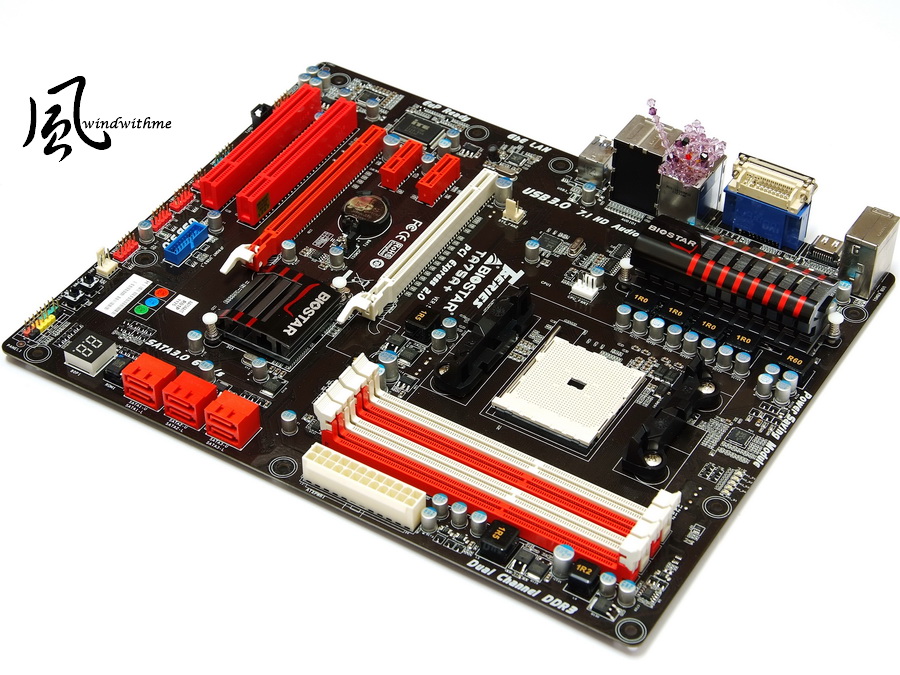 The BIOSTAR TA75A+ costs about US$99(NT$2875) in the U.S. Its BIOS has been upgraded to UEFI interface, with excellent overclocking capacity and debug LED design. It has also been integrated with the original new-era specification of the A75 chipset. It has high competitiveness among the A75 MBs of various brands. However, BIOSTAR still needs to exert effort in terms of increasing its market awareness. In addition, it should be noted that in CPU overclocking, as the A75 chipset increases the CPU 100MHz overclocking, the SATA frequency also increases accordingly. If the CPU overclocking is used for a long time, it is not certain whether it will affect the function of the HDD/SSD when operating with increased frequency. To safely increase the performance of the internal display, the DDR3 frequency should be increased first, and then adjusted to 1600/1866 to achieve stability according to the physical strength of the DDR3. The A75 MB with A8-3850/A6-3650 is an all-in-one platform for the mid-range market. It is highly attractive for users who require high specifications. The major difference with the A55 chipset is the absence of the USB 3.0 and SATA3. But the product is sold at a lower price and it is definitely a valuable option for entry-level computers. Specifically, an earlier model of the A6-3500 or a lower-level of the A4/E4 CPU sells for less the price. When the new-generation APU platform becomes popular in the future, it will be more affordable and valuable. This is good news to consumers who prefer to purchase low-configuration or entry-level computers. This article is also post in my own blog WIND3C Welcome your visit. |
|
|
|
 Similar Threads
 | ||||
| Thread | Thread Starter | Forum | Replies | Last Post |
| The BIOSTAR fair-price TZ68A+ complete analysis | windwithme | Hardware Overclocking and Case Modding | 5 | 28th July 2011 18:28 |
| GIGABYTE A75-UD4H: CrossFire for Llano | jmke | WebNews | 0 | 12th July 2011 13:10 |
| Desktop Llano Overclocking | jmke | WebNews | 0 | 4th July 2011 19:10 |
| The AMD A8-3850 Review: Llano on the Desktop | jmke | WebNews | 1 | 4th July 2011 19:07 |
| AMD Llano hits the mobile market | geoffrey | WebNews | 0 | 16th June 2011 16:32 |
| Socket FM1 the new platform for AMD Llano | jmke | WebNews | 0 | 2nd July 2010 11:54 |
| The complete OC analysis of the AMD Phenom II X6 1090T on ASUS Crosshair IV Formula | windwithme | General Madness - System Building Advice | 5 | 23rd June 2010 17:13 |
| AMD Llano - The First Accelerated Processing Unit | jmke | WebNews | 0 | 19th February 2010 09:48 |
| windwithme's LGA 1156 review part II-Core i5 750 & Biostar TPOWER I55 OC instruction | windwithme | Hardware Overclocking and Case Modding | 4 | 18th September 2009 05:35 |
| AMD Llano - one-die GPU-CPU with DirectX 11 in 2011 | jmke | WebNews | 0 | 7th September 2009 10:16 |
| Thread Tools | |
| |


